


-
What are the TG communication challenges faced by the PCB process?
5G communication has an increasing impact on people’s lives, and newly developed mobile phones will also step into the 5G era little by little. Today, let’s take a look at what challenges 5G communication has brought to the PCB industry! Requirements for materials: A very clear direct...Read more -

How to control the quality of PCBs in PCB Factory?
Quality is the foundation of an enterprise and the hard cornerstone of development. The first pass to ensure quality through strict inspection is to select high-quality plates. If PCB manufacturers want to control the quality of PCBs, how to control it? If we want to control the quality of PCBs, ...Read more -
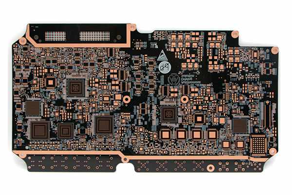
What are the meanings and functions of each layer of PCB?
1. Drilling layer: the drilling layer provides drilling information during the manufacturing process of the PCB (such as pads, vias need to be drilled). 2. Signal layer: the signal layer is mainly used to arrange the wires on the PCB. 3. Solder resist: apply a layer of paint on all parts except t...Read more -
What are the characteristics and types of PCB inks?
PCB ink refers to the ink used in printed circuit boards. Let the PCBFuture share with you what are the characteristics and types of PCB inks? The characteristics of PCB ink (1) Viscosity and Thixotropy In the process of manufacturing printed circuit boards, screen printing is one of the indispen...Read more -

What are the classifications of PCB vias?
Vias is the most common hole in PCB, which mainly plays the role of circuit interconnection and conduction. Vias are traditionally divided into electroplated (supported) holes and non electroplated (unsupported) holes. This is a manufacturing term. For design, holes should be divided into welded ...Read more -

What are the interconnection methods of PCB?
The electronic components and electromechanical components have electrical contacts on the PCB, and the electrical connection between two discrete contacts is called interconnection. So what are the ways of PCB interconnection? Welding method This method has the advantages of simplicity, low co...Read more -
Why is it difficult to tin in PCB pads?
The first reason:We should think about whether it is a customer design problem. It is necessary to check whether there is a connection mode between the pad and the copper sheet, which will lead to insufficient heating of the pad. The second reason : Whether it is a customer operation problem. If...Read more -
What are the special electroplating methods in PCB electroplating?
1. Finger Plating In PCB proofing, rare metals are plated on the board edge connector, board edge protruding contact or gold finger to provide low contact resistance and high wear resistance, which is called finger plating or protruding local plating. The process is as follows: 1) peel off the co...Read more -

What problems should be paid attention to in the etching in PCB proofing?
In PCB proofing, a layer of lead-tin resist is pre-plated on the copper foil part to be retained on the outer layer of the board, that is, the graphic part of the circuit, and then the remaining copper foil is chemically etched away, which is called etching. So, in PCB proofing, what problems sho...Read more -

What matters should be explained to the manufacturer for PCB proofing?
When a customer submits a PCB proofing order, what matters need to be explained to the PCB proofing manufacturer? 1. Materials: explain what kind of materials are used for PCB proofing. The most common is FR4, and the main material is epoxy resin peeling fiber cloth board. 2. board layer: Indica...Read more -
What are the inspection standards in the PCB proofing process?
1. Cutting Check the specification, model and cutting size of the substrate board according to the product processing or cutting specification drawings. The longitude and latitude direction, length and width dimension and perpendicularity of the substrate board are within the scope specified in t...Read more -
How to check after PCB wiring?
After the PCB wiring design is completed, it is necessary to check whether the PCB wiring design conforms to the rules and whether the formulated rules do not conform to the requirements of PCB production process. So, how to check after PCB wiring? These following should be checked after PCB wi...Read more