


In PCB proofing, a layer of lead-tin resist is pre-plated on the copper foil part to be retained on the outer layer of the board, that is, the graphic part of the circuit, and then the remaining copper foil is chemically etched away, which is called etching.
So, in PCB proofing, what problems should be paid attention to in etching?
The quality requirement of etching is to be able to completely remove all copper layers except under the anti-etching layer. Strictly speaking, the etching quality must include the uniformity of the wire width and the degree of side etching.
The problem of side etching is often raised and discussed in etching. The ratio of the side etch width to the etch depth is called the etch factor. In printed circuit industry, a small side etch degree or a low etch factor is the most satisfactory. The structure of the etching equipment and the different compositions of the etching solution will affect the etching factor or side etching degree.
In many ways, the quality of etching exists long before the circuit board enters the etching machine. Because there is a very close internal connection between the various processes of PCB proofing, there is no process that is not affected by other processes and does not affect other processes. Many of the problems identified as etch quality actually existed in the stripping process even earlier.
Theoretically speaking, PCB proofing enters the etching stage. In the pattern electroplating method, the ideal state should be: the sum of the thickness of copper and lead tin after electroplating should not exceed the thickness of the electroplating photosensitive film, so that the electroplating pattern is completely covered on both sides of the film. The “wall” blocks and is embedded in it. However, in actual production, the coating pattern is much thicker than the photosensitive pattern; since the height of the coating exceeds the photosensitive film, there is a trend of lateral accumulation, and the tin or lead-tin resist layer covered above the lines extends to both sides, forming a “Edge”, a small part of the photosensitive film is covered under the “edge”. The “edge” formed by tin or lead-tin makes it impossible to completely remove the photosensitive film when removing the film, leaving a small part of “residual glue” under the “edge”, resulting in incomplete etching. The lines form “copper roots” on both sides after etching, which narrows the line spacing, causing the printed board to fail to meet customer requirements and may even be rejected. The production cost of the PCB is greatly increased due to rejection.
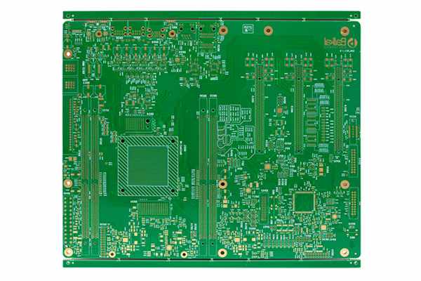
In PCB proofing, once there is a problem with the etching process, it must be a batch problem, which will eventually cause great hidden dangers to the quality of the product. Therefore, it is particularly important to find a suitable PCB proofing manufacturer.
PCBFuture has build our good reputation in the full turnkey PCB assembly service industry for prototype PCB assembly and low volume, mid volume PCB assembly. What our customers need to do is send the PCB design files and requirements to us, and we can take care of the rest of work. We are fully capable of offering unbeatable turnkey PCB services but keeping total cost within your budget.
If you looking for a ideal Turnkey PCB assembly manufacturer, please send your BOM files and PCB files to sales@pcbfuture.com. All your files are highly confidential. We will send you an accurate quote with lead time in 48 hours.
Post time: Dec-09-2022