


1. Drilling layer: the drilling layer provides drilling information during the manufacturing process of the PCB (such as pads, vias need to be drilled).
2. Signal layer: the signal layer is mainly used to arrange the wires on the PCB.
3. Solder resist: apply a layer of paint on all parts except the pad to prevent tin from appearing on these parts, such as solder resist, The solder resist layer is used to match the pads in the design process and is automatically generated.
4. Solder paste protection layer, s-md patch layer: its function is similar to the solder resist layer, except that the surface is bonded to the corresponding pad of the component during machine welding.
5. Prohibited wiring layer: the area where wiring can be effectively placed on the circuit board. Draw a closed area on this layer as the effective area for routing. Generally, it is impossible to automatically layout and route outside this area.
6. Silk screen layer: silk screen layer is mainly used to place printing information, such as outline and mark of components, various annotation characters, etc. Usually, various marking characters are located at the top of the silk screen layer, and the bottom silk screen layer can be closed.
7. Internal power / ground layer: this layer is only used for multilayer boards and is mainly used for arranging power lines and ground wires. We call it double-layer board, four layer board and six layer board, which usually refers to the number of signal layer and internal power / ground layer.
8. Mechanical layer: generally used to set mechanical information such as overall dimensions, data marks, alignment marks and assembly instructions of the circuit board. This information changes according to the requirements of the design company or PCB manufacturer.
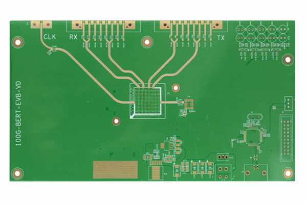
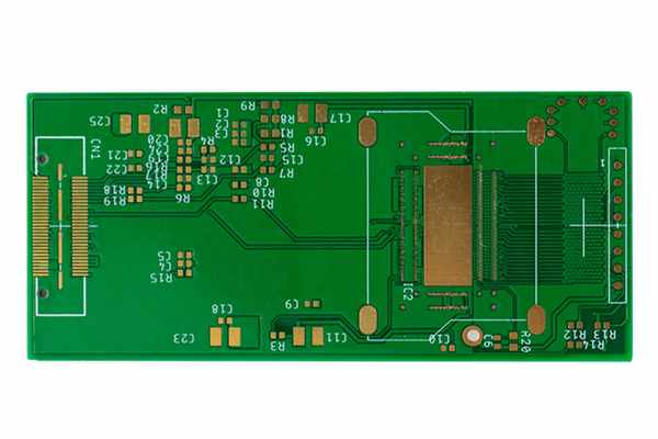
PCBFuture has build our good reputation in the full turnkey PCB assembly service industry for prototype PCB assembly and low volume, mid volume PCB assembly. What our customers need to do is send the PCB design files and requirements to us, and we can take care of the rest of work. We are fully capable of offering unbeatable turnkey PCB services but keeping total cost within your budget.
If you looking for a ideal Turnkey PCB assembly manufacturer, please send your BOM files and PCB files to sales@pcbfuture.com . All your files are highly confidential. We will send you an accurate quote with lead time in 48 hours.
Post time: Mar-03-2023