


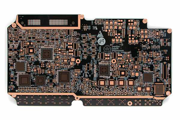
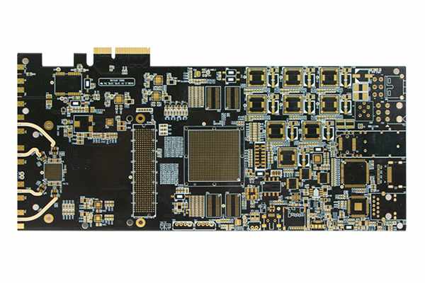
5G communication has an increasing impact on people’s lives, and newly developed mobile phones will also step into the 5G era little by little. Today, let’s take a look at what challenges 5G communication has brought to the PCB industry!
Requirements for materials:
A very clear direction for 5G PCB is high-frequency and high-speed materials and boards. Wu Jun pointed out that in terms of high-frequency materials, it is obvious that leading material manufacturers in the traditional high-speed field, such as Lianmao, Shengyi, and Panasonic, have begun to deploy high-frequency boards and launched a series of new materials. This will break the current situation of Rogers’ dominance in the field of high-frequency sheets. After healthy competition, the performance, convenience and availability of materials will be greatly enhanced. Therefore, the localization of high-frequency materials is an inevitable trend.
 Requirements for quality monitoring:
Due to the increase in the 5G signal rate, the deviation of the board making has a greater impact on the signal performance, which requires stricter control of the production deviation of the board making, and the existing mainstream board making processes and equipment are not updated much, will become the bottleneck of future technological development. It is very important for PCB manufacturers to break the situation.
In terms of quality control, PCBFuture has strengthened the statistical process control of key product parameters on the basis of the original. More real-time management of data ensures the consistency of products to meet the performance requirements of the antenna in terms of phase, standing wave, and amplitude.
Requirements for process technology:
The functional improvement of 5g related application products will increase the demand for high-density PCB, and HDI will also become an important technical field. Multi stage HDI products and even products interconnected in any order will be promoted, and new technologies such as buried resistance and buried capacity will be more and more applied.
The copper thickness uniformity, line width accuracy, interlayer alignment, interlayer medium thickness, control accuracy of back drilling depth and plasma decontamination ability of PCB are worthy of further study.
 Requirements for equipment and instruments:
High precision equipment and pretreatment line with less roughening of copper surface are ideal processing equipment at present. The test equipment includes passive intermodulation tester, flying pin impedance tester, loss test equipment and so on.
Precision pattern transfer and vacuum etching equipment, which is a detection equipment that can monitor and feedback the line width and coupling spacing of data changes in real time. Electroplating equipment with good uniformity and high-precision laminating equipment can also meet the production requirements of 5g PCB.
At a time when the PCB industry is facing great challenges, PCBFuture will not be afraid to move forward to meet the higher needs of customers. We are look forward to working with you for the PCB assembly projects. For more information, please email to service@pcbfuture.com.
Post time: Mar-29-2023