


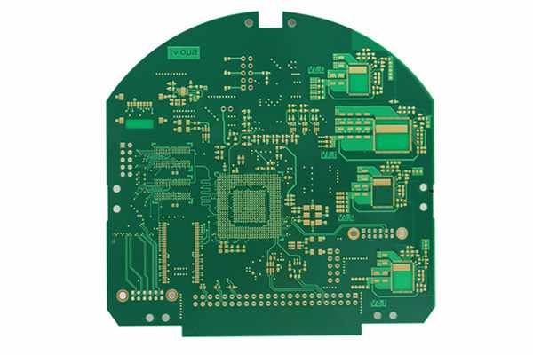
Vias is the most common hole in PCB, which mainly plays the role of circuit interconnection and conduction. Vias are traditionally divided into electroplated (supported) holes and non electroplated (unsupported) holes. This is a manufacturing term. For design, holes should be divided into welded and non welded.
1. Welded vias
Except that the external surface area must be large to enhance heat dissipation to avoid the problem of poor welding, most of the rules apply to the through hole to be welded. For consistency and ease of calculation, unless simplified pads are required, the inner pads should be the same as the outer pads.
2. Not welded vias
The designer must first know whether the pad is welded or not. This information can help the engineer decide whether the pad is for welding or for the smallest hole ring. It is important to note whether the pads are plated or not. In the plating process, if the pads exist, the holes are plated with copper foil. If the pads are not plated, they must be drilled after the plating process.
(1) Non plated vias with pad
Non plated vias refers to non plating in the hole through the pad. This means that there is no additional carrier to support the pads in addition to the normal copper adhesive. For this reason, the pads must be large enough to facilitate bonding and support the pads during heating or welding.
(2) Non plated vias, no pad
The general NPTH is as large as the non pad or the hole plated on the hole wall on a printed board, such as the mounting hole, the screw adjustment access hole, the wire transfer hole, etc. Non plating or hole ring requirements are required, and the universal vias is different from other holes because it is not plated or soldered.
PCBFuture has build our good reputation in the full turnkey PCB assembly service industry for prototype PCB assembly and low volume, mid volume PCB assembly. What our customers need to do is send the PCB design files and requirements to us, and we can take care of the rest of work. We are fully capable of offering unbeatable turnkey PCB services but keeping total cost within your budget.
If you looking for a ideal Turnkey PCB assembly manufacturer, please send your BOM files and PCB files to sales@pcbfuture.com. All your files are highly confidential. We will send you an accurate quote with lead time in 48 hours.
Post time: Feb-16-2023