


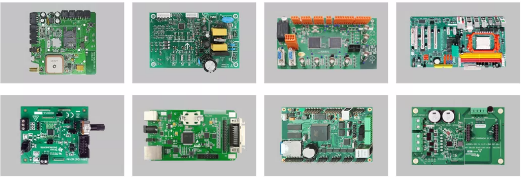
The problems should be paid attention when plug components in PCB Assembly process
The components of PCB should be correctly selected on the premise of meeting the circuit function requirements. It should be noted that the sensitive voltage threshold of components with the same function, model and different suppliers may have great differences. So, what problems should we pay attention to when inserting components in PCB?
1. Limit output current to avoid lock effect of CMOS circuit
The lock-in effect is a special failure mode of CMOS circuit, because there are parasitic PNP transistor and NPN transistor in the internal structure of CMOS circuit, and they form a parasitic PNPN thyristor structure, so the lock-in effect of CMOS circuit is also called “thyristor effect”.
2. Using filter networks
Sometimes a long input cable is needed between the CMOS circuit system and the mechanical contact, which increases the possibility of electromagnetic interference. So, filter network should be considered.
3. RC network
Where it is feasible, for the sensitive input of bipolar devices, the RC network composed of resistors with larger resistance and capacitors with at least 100pF can reduce the influence of electrostatic discharge.
4. Avoiding the pin of input tube for CMOS is suspended.
Avoid that the input end of CMOS device soldered on the circuit board is suspended. At the same time, it should be pay attention to all unnecessary input leads on the CMOS device are not allowed to be suspended. Because once the input is suspended, the input potential will be in an unstable state.
The above is a summary of the problems that should be paid attention to in the process of inserting components into PCB. I hope that it will be helpful to you. For more details, please visit our website www.pcbfuture.com
Post time: May-14-2021