


16 type of common PCB soldering defects
In PCB assembly process, a variety of defects often appear, such as false soldering, overheating, bridging and so on. Below PCBfuture will explain the normal PCB assembly defects when solder the PCBs and how to avoid it.
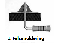
1. False soldering
Appearance features: there is obvious black boundary between solder and component lead, or copper foil, and solder is concave to the boundary.
Harm: not working properly.
Reason: the lead of components is not cleaned, tin is not plated or tin is oxidized. The printed circuit board is not cleaned, and the quality of spraying flux is not good.
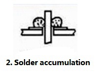
2. Solder accumulation
Appearance features: the solder joint structure is loose, white and lusterless.
Harm: insufficient mechanical strength may cause false welding.
Reason: poor solder quality. The welding temperature is not enough. When the solder is not solidified, the component lead is loose.
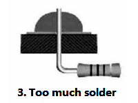
3. Too much solder
Appearance features: the solder surface is convex.
Harm: solder is wasted and defects may not be easily seen.
Reason: incorrect operation during soldering.
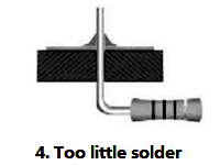
4. Too little solder
Appearance features: the welding area is less than 80% of the pad, and the solder does not form a smooth transition surface.
Harm: insufficient mechanical strength.
Reason: solder mobility is poor or premature solder withdrawal. Insufficient flux. The welding time is too short.
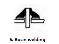
5. Rosin welding
Appearance features: there is rosin slag in the weld.
Harm: insufficient strength, poor conduction, sometimes on and off.
Reason: there are too many welding machines or welder failure. Insufficient welding time and heating. The surface oxide film was not removed.
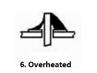
6. Overheated
Appearance features: white solder joint, no metallic luster, rough surface.
Harm: the pad is easy to peel off and the strength is reduced.
Reason: the power of the soldering iron is too large, and heating time is too long.
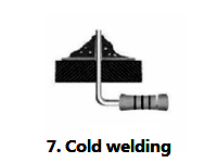
7. Cold welding
Appearance features: The surface is granular, and sometimes there may be cracks.
Harm: Low strength and poor conductivity.
Reason: the solder is shaken before it solidifies.
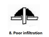
8. Poor infiltration
Appearance features: the interface between solder and weldment is too large and not smooth.
Harm: low strength, no access or time-on and off.
Reason: the weldment is not cleaned up. Flux is insufficient or poor quality. The weldment is not fully heated.
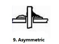
9. Asymmetric
Appearance features: solder doesn’t flow over the pad.
Harm: Insufficient strength.
Reason: the solder has poor fluidity. Insufficient flux or poor quality. Insufficient heating.
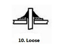
10. Loose
Appearance characteristics: The wire or component lead can be moved.
Harm: poor or non-conduction.
Reason: before the solder solidifies, the lead wire moves to cause voids. The lead is not processed well.
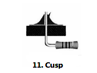
11. Cusp
Appearance characteristics: sharp.
Harm: poor appearance, easy to cause bridging
Reason: too little flux and too long heating time. The leaving angle of the soldering iron is improper.
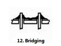
12. Bridging
Appearance characteristics: adjacent wires are connected.
Harm: Electrical short circuit.
Reason: too much solder. Improper angle of retraction of soldering iron.
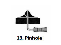
13. Pinhole
Appearance features: visual inspection or low-power amplifiers can see holes.
Harm: insufficient strength, solder joint easy to corrode.
Reason: the gap between the lead and the pad hole is too large.
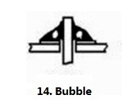
14. Bubble
Appearance features: there is a fire-breathing solder bulge at the root of the lead, and a cavity is hidden inside.
Harm: temporary conduction, but it is easy to cause poor conduction for a long time.
Reason: the gap between the lead and the welding disc hole is large. Poor lead infiltration. The welding time of double-sided plugging through holes is long, and the air in the holes expands.
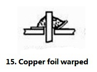
15. Copper foil warped
Appearance features: the copper foil is peeled off from the printed board.
Harm: PCB is damaged.
Reason: the welding time is too long and the temperature is too high.
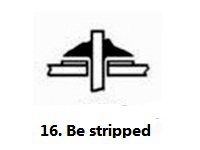
16. Be stripped
Appearance characteristics: the solder joints peel off from the copper foil (not copper foil and PCB).
Harm: Open circuit.
Reason: bad metal coating on pad.
PCBFuture provide all inclusive PCB assembly services, including PCB manufacturing, component sourcing and PCB assembly. Our Turnkey PCB service eliminates your need to manage multiple suppliers over multiple time frames, resulting in increased efficiency and cost effectiveness. As a quality driven company, we fully respond to the needs of customers, and can provide timely and personalized services that large companies cannot imitate. We can help you avoid the PCB soldering defects in your products.
Post time: Nov-06-2021