


Why should we plug the vias in the PCB?
In order to meet the requirements of customers, the via holes in circuit board must be plugged. After a lot of practice, the traditional aluminum plug hole process is changed, and the white net is used to complete the resistance welding and plug hole of circuit board surface, which can make the production stable and the quality reliable.
Via hole plays an important role in the interconnection of circuits. With the development of electronic industry, it also promotes the development of PCB, and puts forward higher requirements for PCB fabrication and assembly technology. Via hole plug technology came into being, and the following requirements should be met:
(1) The copper in the via hole is enough, and the solder mask can be plugged or not;
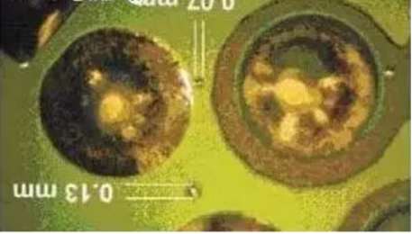
(2) There must be tin and lead in the via hole, with a certain thickness requirement (4 microns), no solder resist ink into the hole, causes tin beads to be hidden in the holes;
(3) There must be solder resistance ink plug hole in the via hole, which is not transparent, and there must be no tin ring, tin beads and flat.
 With the development of electronic products in the direction of “light, thin, short and small”, PCB also developing towards high density and high difficulty. Therefore, a large number of SMT and BGA PCBs have appeared, and customers require plugging holes when mounting components, which mainly have five functions:
(1) In order to prevent short circuit caused by tin penetrating through the element surface during PCB over wave soldering, especially when we place the through hole on the BGA pad, we must first make the plug hole and then gold plating to facilitate BGA soldering.
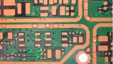
(2) Avoid flux residue in the via holes;
(3) After the surface mount and component assembly of the electronics factory, the PCB should absorb vacuum to form negative pressure on the testing machine;
(4) Prevent the surface solder from flowing into the hole, and causing false soldering and affecting the mount;
(5) prevent the solder bead from popping out during the wave soldering, and causing short circuit.
Realization of plug hole technology for via hole
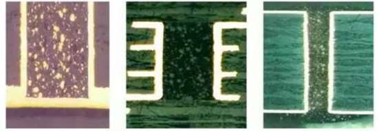
For SMT PCB assembly board, especially the mounting of BGA and IC, the via hole plug must be flat, the convex and concave plus or minus 1mil, and there must be no red tin on the edge of the via hole; in order to meet the customer’s requirements, the through hole plug hole process can be described as multifarious, long process flow, difficult process control, there are often problems such as oil drop during hot air leveling and green oil solder resistance test and oil explosion after curing. According to the actual conditions of production, we summarize the various plug hole processes of PCB, and makes some comparison and elaboration in the process and advantages and disadvantages:
Note: the working principle of hot air leveling is to use hot air to remove the excess solder on the surface of printed circuit board and in the hole, and the remaining solder is evenly covered on the pad, non blocking solder lines and surface packaging points, which is one of the ways of surface treatment of printed circuit board.
1. Plug hole process after hot air leveling: plate surface resistance welding → HAL → plug hole →curing. The non-plugging process is adopted for production. After hot air leveling, aluminum screen or ink blocking screen is used to complete the through hole plug of all fortresses required by customers. Plug hole ink can be photosensitive ink or thermosetting ink, in the case of ensuring the same color of wet film, the plug hole ink is best to use the same ink as the board. This process can ensure that the through hole will not drop oil after hot air leveling, but it is easy to cause the plug hole ink to pollute the plate surface and uneven. It is easy for customers to cause false soldering during mounting (especially BGA). So, many customers don’t accept this method.
2. Plug hole process before hot air leveling: 2.1 plug hole with aluminum sheet, solidify, grind the plate, and then transfer the graphics. This process uses CNC drilling machine to drill out the aluminum sheet that needs to be plugged hole, make screen plate, plug hole, ensure the through hole plug hole full, plug hole ink, thermosetting ink can also be used. Its characteristics must be high hardness, small shrinkage change of resin, and good adhesion with hole wall. The technological process is as follows: pretreatment → plug hole → grinding plate → pattern transfer → etching → plate surface resistance welding. This method can ensure that the through hole plug hole is smooth, and hot air leveling will not have quality problems such as oil explosion and oil dropping at the hole edge. However, this process requires one-time thickening of copper to make the copper thickness of the hole wall meet the customer’s standard. Therefore, it has high requirements for copper plating of the whole plate and the performance of the plate grinder, so as to ensure that the resin on the copper surface is completely removed, and the copper surface is clean and not polluted. Many PCB factories don’t have one-time thickening copper process, and the performance of the equipment can’t meet the requirements, so this process is rarely used in PCB factories.
(The blank silk screen) (The stall point film net)
We are helpful, attentive and supportive with a proactive approach to help you win in competitive markets. For more information, please email to service@pcbfuture.com.
Post time: Jul-01-2021