


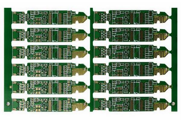
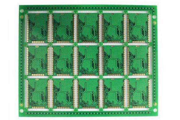
In order to improve production efficiency and reduce production cost in PCB assembly process, bare circuit boards usually make in panel for production, which can facilitate PCBA processing plant to carry out chip welding. The following will talk about the common panelized methods and principles of circuit board.
Principle of PCB panelization:
1. The size of PCB panel board width ≤ 300mm (Fuji line); if need automatic dispensing , the size of PCB should ≤ 125mm(W) × 180mm(L).
2. The shape of PCB shall be close to the square as far as possible, and recommended the splicing board is (2*2、3 *3、4* 4) in each panel.
3. The outer frame (clamping edge) of circuit board shall adopt closed-loop design to ensure that the PCB panel will not deform after it is fixed on the fixture.
4. The small PCB board center distance shall be controlled in 75mm~145mm.
5. There shall be no large devices or protruding devices near the connection point between the outer frame of the splicing board and the internal small board, and there shall be a space greater than 0.5mm between the components and the edge of the PCB board to ensure the normal operation of the cutting tool.
6. At the four corners of PCB’s outer frame, four positioning holes are opened and the hole diameter is (4mm ± 0.01mm); The strength of the hole shall be moderate to ensure that it will not break during the process of loader and unloader; The hole diameter and position accuracy shall be high, and the hole shall be smooth.
7. Each small board in the PCB must have at least three positioning holes, 3 ≤ hole diameter ≤ 6mm, and wiring or SMT is not allowed within 1mm of the edge positioning hole.
8. When setting the reference positioning point, a non resistance welding area 1.5mm larger than the positioning point is usually reserved around the positioning point.
9. Large components shall be provided with positioning posts or positioning holes, such as: microphone, battery interface, microswitch, headset interface, motor, etc.
The common PCB connected ways in panel:
1、V-CUT
V-CUT means that several boards or the same board can be combined and spliced together, and then a V-groove can be cut with a V-CUT machine between boards after PCB processing, which can be broken during use. It is a more popular way nowadays.
2. Punching groove
Punching refers to milling empty between plates or inside plates with a milling machine as required, which is equivalent to digging out.
3. Stamp hole
This means use small hole to link the PCB board, which looks like the sawtooth shape on the stamp, so it is called stamp hole link. The stamp hole link requires high control burr around the board, that is only a little stamp hole can be used to replace the V line.
Want to know more, please click : www.PCBfuture.com
Post time: Jan-13-2022