


We often encounter poor BGA soldering in the process of PCB assembly process due to improper PCB design in the work. Therefore, PCBFuture will make a summary and introduction to several common design problem cases and I hope it could provide valuable opinions for PCB designers!
There are mainly the following phenomenas:
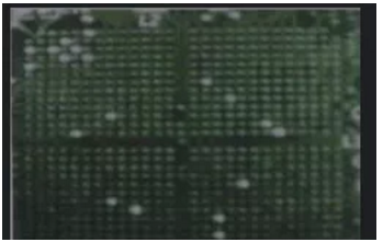
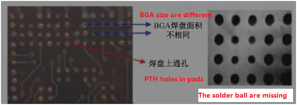
1. The bottom vias of the BGA are not processed.
There are via holes in the BGA pad, and the solder balls are lost with the solder during the soldering process; The PCB manufacturing does not implement the solder mask process, and causes the loss of solder and solder balls through the vias adjacent to the pad, resulting in the solder balls missing, as shown in the following picture.
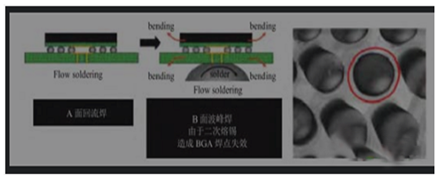
2.The BGA solder mask is poorly designed.
The placement of via holes on the PCB pads will cause solder loss; The high-density PCB assembly must adopt microvia, blind vias or plugging processes to avoid solder loss; As shown in the following picture, it uses wave soldering, and there are vias at the bottom of the BGA. After wave soldering, the solder on the vias affects the reliability of BGA soldering, causing problems such as short circuits of components.
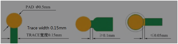
3. The BGA pad design.
The lead wire of the BGA pad should not exceed 50% of the diameter of the pad, and the lead wire of the power supply pad should not be less than 0.1mm, and then thicken it. In order to prevent deformation of the pad, the solder mask window should not be larger than 0.05mm, as shown in the following picture.
4. The size of the PCB BGA pad is not standardized and it is too large or too small, as shown in the figure below.
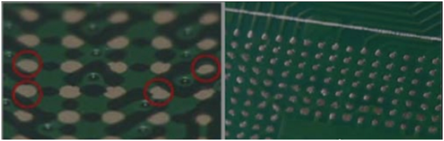
5. The BGA pads have different sizes, and the solder joints are irregular circles of different sizes, as shown in the figure below.
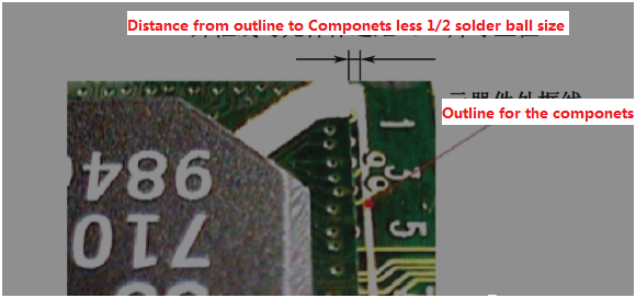
6. The distance between the BGA frame line and the edge of the component body is too close.
All parts of the components should be within the marking range, and the distance between the frame line and the edge of the component package should be more than 1/2 of the solder end size of the component, as shown in the figure below.
PCBFuture are a professional PCB & PCB assembly manufacturer who can provide with PCB manufacturing, PCB assembly and components sourcing services. The perfect quality assurance system and various inspection equipments help us to monitor the whole production process, assure stability of this process and high product quality, meanwhile, advanced instruments and technology methods have been introduced to attain sustained improvement.
Post time: Feb-02-2021